PCB is one of the essential main components used in all electronic devices.
It is a complex component that connects the circuits of various and numerous components.
Among these, we will learn about soldering and soldering cracks that connect the PCB and components.
Soldering is used to connect the pads of the PCB and the terminals of the components in order to connect the components on the PCB. You may have seen soldering with a wire that looks like thread at least once.
However, most electronic products these days are soldered using automated machines.

Soldering is done through automated equipment for uniform, large-scale soldering.
It is called SMT (Surface mount technology) and SMD (Surface mount device).
In automated SMT, solder paste (small granules of solder cream) is applied to the pads of the PCB using automated equipment and components are placed on top of it. After that, the solder is set to a temperature that melts like baking a pizza, and then the PCB passes through. If you have seen a pizza being baked in bulk, you will understand it roughly.
Since many PCBs pass through at once for soldering, it is also called reflow soldering.
In the past, tin (Sn) alloy containing lead (Pb) was used a lot as a material used in soldering. This is because it has a relatively low melting point (approximately 183 degrees) and is a common material.
However, due to the harmfulness of lead (Pb), Pb-free became essential, and solder containing lead (Pb) is rarely used in recent electronic products.
Therefore, solder containing tin (Sn) is used these days. Generally, the material called SAC 305 (Sn, Ag3.0%, Cu0.5%) is the most used. It has a relatively high melting point (approximately 230 degrees), but is free from harmfulness and is inexpensive.
Soldering completed like this is not completely stable. Defects can occur during soldering, and even if soldering is completed well, failures can occur later.
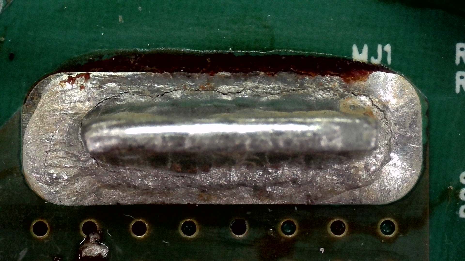
Here, let's first look at the cracks that occur after soldering.
Various materials are used in PCBs. The raw materials, which are PCB insulating boards made of resin+filler (also called prepreg),and the copper-plated circuits are composed. The pads and various components connected to each circuit are soldered and composed. (MLCC, Resistor, Diode, IC, etc.)

Do you know the environment in which electronic devices using PCBs completed like this operate? There are cold places and hot places. There are also cases where they move back and forth from cold to hot places. In such an environment, the PCB is stressed.
Have you ever heard the saying, 'All substances expand when heated'?
Literally, all substances are made of atoms. Atoms are always vibrating slightly, and when the temperature rises, this vibration becomes more severe and the gap between atoms increases. So they expand.
Literally, all substances are made of atoms. Atoms are always vibrating slightly, and when the temperature rises, this vibration becomes more severe and the gap between atoms increases. So they expand. This phenomenon is called thermal expansion, and the coefficient of thermal expansion (CTE) is the degree of thermal expansion of each material.
First, I mentioned that various materials are used in PCBs. Insulating substrates made of polymer materials for insulation, copper for conducting electricity, various surface treatments (plating, etc.) to protect the copper, and the components of the components... There are countless materials used. This means that all of these materials have different coefficients of thermal expansion.
Let's assume that the PCB, which is made up of such complex materials, operates in an environment where the temperature is 100 ℃ or higher, and then the electronic product operates in an environment where the temperature drops again.
All the parts and elements that make up the PCB repeat expansion and contraction. During this process, a lot of stress accumulates in the soldering area where different materials are joined.
If the stress is continuously repeated, cracks will occur in the weakest solder among the joints that are joined with other materials. The user may not notice it because the electronic product is working well right now. However, the stress will continue to repeat, and as a result, the crack will gradually spread and expand from the point where the crack started. As a result, the solder crack will occur throughout the joint, causing the electronic product to fail.

There are several ways to inspect these solder cracks. If the solder area is exposed, it can be detected to some extent through an external microscope inspection, and for parts such as BGA ICs that are not exposed, a destructive inspection (cross-ectional inspection, section) may be necessary. Ink penetration (Dye & Pry) inspection is also performed to check the overall soldering status of the BGA component.
Solder cracks like this are likely to occur when the PCB or component is overheated. They are even more likely to occur in harsh operating environments such as automobiles, military, and aviation parts.
That's why many researchers at automakers, parts makers, military and aerospace manufacturers are conducting numerous reliability tests and analyses in advance to prevent and detect such defects in advance.